比利时微电子研究中心Thierry Conard博士和Clement Merckling博士来苏州纳米所访问交流
11月28日,应纳米真空互联实验站李坊森副研究员邀请,比利时微电子研究中心(IMEC)Thierry Conard 博士和Clement Merckling博士来苏州纳米所进行学术交流,分别作了题为“Surface analysis in the semiconductor industry: Present need and future directions”和“Exploratory materials grown by MBE @ imec”的学术报告,学术交流会由丁孙安研究员主持。
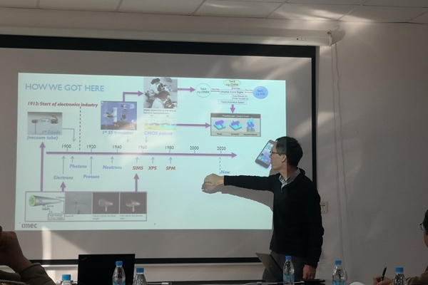
Thierry介绍了XPS以及SIMS的相关研究,这两种设备用于研究二维材料以及多层薄膜结构。利用不同靶的XPS测试同一多层薄膜的不同元素的结合能的信号强度。此外还利用SIMS和探针设备原位研究SIMS测试薄膜后的形貌。
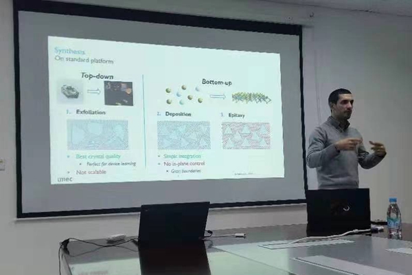
Clement介绍用分子束外研设备外延薄膜的研究。利用范德瓦尔斯结合力研究拓扑材料以及二维材料的生长,研究衬底表面处理以及处理后的外延薄膜的孪晶和衬底之间的关系,此外也研究了在硅衬底上外延氧化物一级组分调制的氧化物薄膜,并展示了外延氧化物薄膜薄膜的压力响应特性。
Thierry Conard博士和Clement Merckling博士的报告内容丰富多彩,为参加本次学术报告会的人员拓展了视野。报告后,对老师和学生们的问题进行了耐心详细的解答,聆听此次报告的师生们表示报告十分精彩、收获颇丰。
简介:
IMEC is a world-leading R&D and innovation hub in nanoelectronics and digital technologies. The combination of widely acclaimed leadership in microchip technology and profound software and ICT expertise is what makes them unique. By leveraging their world-class infrastructure and local and global ecosystem of partners across a multitude of industries, they create groundbreaking innovation in application domains such as healthcare, smart cities and mobility, logistics and manufacturing, energy and education.
Thierry Conard obtained his PhD in 1994 on the growth and characterization by electron spectroscopies of epitaxial copper oxide from the University of Namur in Belgium. He then joined Waseda University in Tokyo, Japan for 2 years where he continued his work on electron spectroscopies on hexagonal Boron Nitride.
In 1996 he started in Imec as a researcher on XPS and TOF-SIMS, in charge of building the service activities in these domains for supporting the imec process development in the area of semiconductor technology. In 2005 he became team leader from the team responsible of the photoemission (including synchrotron), TOFSIMS, EDS (SEM) and AES activities as a service. In this time he also continued his research activities in surface science and the development of surface science as a metrology techniques, focusing among other on Angle resolved XPS and introducing 3D-TOFSIMS and HAXPES in Imec. This leads to about 300 publications as author or co-author and he became Principle Member of Technical Staff function in 2019.
Clement Merckling obtained in 2007 a PhD in Material Sciences from the Ecole Centrale de Lyon in France. His PhD thesis between INL/CNRS laboratory and ST Microelectronics company was focused on the Molecular Beam Epitaxy (MBE) of oxides on Si substrates for high-k gate dielectrics in advanced CMOS devices.
During the period 2007 - 2013, he worked as scientist and then as senior scientist, driving the Molecular Beam Epitaxy (MBE) activities @ imec including III-V semiconductors heteroepitaxy, high-k oxide growth and passivation studies for high-m channels (III-V & GeSn).
In 2013, as a principal member of technical staff, he took the technical lead of III-V epitaxy activities for the IMEC Logic and Photonic programs, focusing on the selective area growth of III-V compounds on Silicon by Vapor Phase Epitaxy (MOVPE). Through the fundamental understanding of the heteroepitaxial processes, world-first III-V FinFET devices and III-V Laser devices monolithically integrated on Silicon were demonstrated at IMEC.
Since 2018, he is focusing on exploratory materials grown by MBE and Pulsed Laser Deposition (PLD) for beyond CMOS devices.
 Thierry Conard博士作报告
 Clement Merckling博士作报告
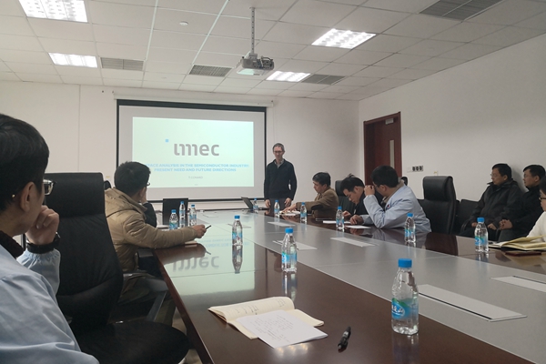
 会议现场
会议现场
附件下载:

